The race for Artificial Intelligence is usually explained through names such as NVIDIA, TSMC, Microsoft, Google and Amazon. Some design accelerators, others manufacture them, while the major cloud providers install thousands of them in data centres. Yet all this computing capacity depends on an earlier and far less visible technology: the machines capable of transferring increasingly small circuits onto a silicon wafer.
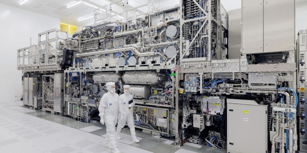
Much of this technology comes from Veldhoven, in the Netherlands (Europe), where ASML is headquartered. The company does not manufacture chips or develop Artificial Intelligence models, but it supplies the lithography systems used by leading manufacturers to produce the most advanced semiconductors. Its position helps explain why digital infrastructure begins long before the server, the data centre or the cloud.
ASML: the key facts in 20 seconds
- ASML was founded in 1984 as a joint venture between Philips and ASM International.
- It manufactures lithography systems that project circuit patterns onto silicon wafers.
- It is the only supplier of extreme ultraviolet lithography systems, known as EUV, used in high-volume manufacturing.
- Its equipment is installed in semiconductor plants operated by companies such as TSMC, Samsung, Intel and SK hynix.
- It also manufactures DUV systems, which are required for many chip layers and a wide range of semiconductor products.
- In 2025, it reported net sales of €32.7 billion and net income of €9.6 billion.
- During the first quarter of 2026, it generated sales of €8.8 billion, net income of €2.8 billion and a gross margin of 53%.
- ASML expects to close 2026 with revenue of between €36 billion and €40 billion.
- Its next-generation technology, High-NA EUV, increases numerical aperture from 0.33 to 0.55 and can print smaller structures.
- Its strategic importance has also placed it at the centre of export controls and technological competition between the United States, China, Europe and Asia.
These figures reveal an industrial company in a highly unusual position. In 2025, ASML invested €4.7 billion in research and development. It also generated €8.2 billion from services, maintenance and upgrades for equipment already installed, 26.2% more than in the previous year. ASML does not depend solely on selling new machines: it maintains technical relationships that can last for decades with the factories using its systems.
Demand linked to Artificial Intelligence has strengthened this business. Large models require accelerators, but also high-bandwidth memory, processors, networking components and high-speed interconnects. To increase production, logic and memory manufacturers must expand their fabrication plants, install new machines and upgrade existing equipment.
This does not mean that every chip used for Artificial Intelligence is manufactured exclusively with EUV equipment. Semiconductor production combines numerous processes and technologies. ASML maintains an extensive DUV portfolio based on deep ultraviolet light, which remains essential for many chip layers, mature process nodes and components where using the most advanced tool would make little economic sense.
EUV and DUV will coexist for many years. A semiconductor plant may use EUV for its most complex structures while relying on DUV for many other exposures. This combination explains why ASML’s position extends beyond the latest processors to memory, industrial electronics, automotive systems, communications and many everyday devices.
How EUV lithography works and why it is so difficult to replicate
Lithography can be compared to an extraordinarily precise form of photographic printing. The process begins with a silicon wafer covered in a light-sensitive material. The machine projects the pattern corresponding to one circuit layer onto the wafer. Chemical and physical processes are then applied to etch, deposit or alter materials.
This operation is repeated many times. A modern chip consists of successive layers that must be aligned with extreme precision. A minor error can affect the yield of the entire wafer and reduce the percentage of chips that function correctly.
Complete semiconductor production involves hundreds of steps and may take several months. Lithography is only one of them, but it directly influences feature size, transistor density and the economic viability of the manufacturing process.
ASML’s EUV machines use light with a wavelength of 13.5 nanometres. To produce it, a carbon dioxide laser fires two pulses at tiny droplets of tin moving through the system. The tin is converted into plasma and emits extreme ultraviolet radiation. The machine can repeat this operation up to 50,000 times per second.
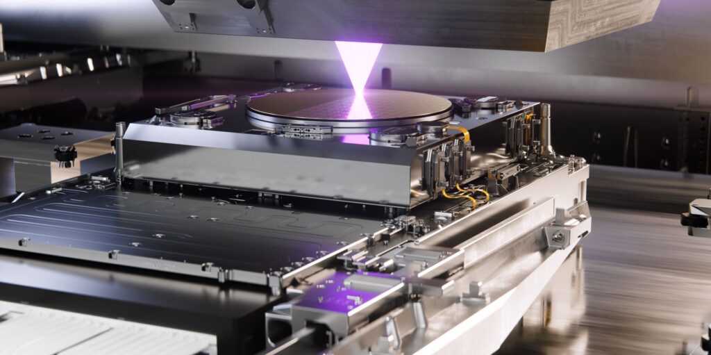
This creates another difficulty. EUV light is absorbed by almost every material, including air. It cannot pass through conventional glass lenses, so the entire optical path must operate in a vacuum and use highly precise multilayer mirrors.
These mirrors are supplied by ZEISS Semiconductor Manufacturing Technology, one of ASML’s most important partners. The optical systems must direct and focus the light while the wafer and mask move at high speed. At the same time, the machine uses sensors and software to correct vibration, temperature changes, positioning and potential deviations.
The illumination optics of a conventional EUV system already contain around 15,000 components and weigh approximately 1.5 tonnes. In High-NA EUV, the illumination system includes more than 25,000 components and weighs over six tonnes. Its mirrors are manufactured with atomic-level precision, and some can take about a year to produce.
ASML therefore acts as the integrator of an international technological system. In addition to ZEISS, the platform depends on laser sources, vacuum systems, metrology, materials, software and components developed by a network of specialist suppliers. ASML controls the overall architecture and coordinates the system’s operation inside its customers’ semiconductor plants.
This specialisation explains why its position is so difficult to replicate. A competitor would not merely have to copy a single machine. It would need to rebuild decades of expertise in optics, plasma generation, mechanics, materials, motion control, manufacturing and software. It would also have to create a network of suppliers and work for years with semiconductor manufacturers to turn prototypes into reliable tools for continuous production.
The development of EUV required more than two decades, thousands of professionals and billions of euros in research. ASML estimates that it invested more than €6 billion in the technology over 17 years before it reached the level of maturity required for large-scale manufacturing. The company also acquired Cymer, a specialist in light sources, to accelerate progress in one of the system’s most complex areas.
The next stage is High-NA EUV. The term refers to a higher numerical aperture, which improves the optical system’s ability to collect and focus light. ASML’s EXE platform increases this value from 0.33 to 0.55.
According to the manufacturer’s specifications, the TWINSCAN EXE:5000 achieves a resolution of eight nanometres. It can print features 1.7 times smaller than NXE platforms in a single exposure and potentially increase transistor density by up to 2.9 times. The first machine was shipped to Intel at the end of 2023, and ASML recognised revenue associated with four EXE systems during 2025.
Adoption will not be automatic or identical for every manufacturer. Each company must assess the cost of the machine, its productivity, the number of exposures it can eliminate, process maturity and the resulting wafer yield. A more advanced technology is useful only when it improves the economics of the complete fabrication process.
From Veldhoven to the data centre
The connection between ASML and cloud infrastructure may appear distant, but it links two ends of the same chain. Lithography systems make it possible to manufacture processors, accelerators and memory. These components are then integrated into servers, storage platforms and networking equipment. Finally, data centres turn that hardware into computing capacity that companies and users can consume.
When a new manufacturing generation increases transistor density, improves performance or reduces energy consumption per operation, the effect eventually reaches the data centre. Providers can install more capacity within the same physical space, offer more powerful servers or run certain workloads with a better balance between performance and electricity consumption.
The process is not immediate, however. Between a lithography advance and its arrival in business infrastructure lie chip design, process validation, manufacturing, packaging, server integration and commercial availability. Announcements about new semiconductor nodes should therefore not be confused with capacity that can be deployed immediately.
Demand also flows in the opposite direction. Growth forecasts for Artificial Intelligence are leading data centre operators and hyperscalers to reserve large volumes of accelerators. Chip designers pass that demand on to foundries, which increase their investment in capacity and manufacturing equipment. ASML benefits from this cycle without selling servers or cloud services directly.
For companies consuming infrastructure, this supply chain has practical consequences. The availability and price of certain processors may depend on bottlenecks located thousands of kilometres away from the data centre. There can also be substantial differences between hardware generations in power consumption, density, performance per core and memory capacity.
In private cloud and bare-metal environments, hardware selection directly affects platform design and total cost of ownership. A company does not always need the newest CPU or the most powerful accelerator. It must choose the architecture that best matches its databases, virtualisation requirements, Artificial Intelligence workloads, storage, latency and expected growth.
Bare-metal environments allow the processor, memory, storage and network to be dedicated to a single organisation. This provides isolation, predictable performance and direct control of the hardware. Private cloud adds a layer of virtualisation, automation and management that makes it easier to distribute these resources among virtual machines and internal services.
From the perspective of a European provider such as Stackscale, semiconductor innovation is one part of the challenge, but it does not solve enterprise infrastructure requirements on its own. High availability, private networks, backups, storage, monitoring, disaster recovery and day-to-day operations must also be designed properly.
A new CPU may reduce processing times, but it does not replace a business continuity plan. An accelerator may run Artificial Intelligence models quickly, but it does not determine where the data is stored, who operates the platform or which jurisdiction governs the provider. Performance, resilience and sovereignty are related but distinct considerations.
ASML also helps to put European technological sovereignty into perspective. The company retains in the Netherlands a capability that no other supplier has managed to reproduce commercially. Europe therefore holds a strategic position within the global semiconductor manufacturing industry.
However, ASML does not represent a completely autonomous European supply chain. Its machines incorporate technology and components from several countries. Its main customers manufacture in Taiwan, South Korea and the United States. The company relies on ZEISS in Germany, US specialists and an international network of suppliers.
Its strength comes precisely from this cooperation. At the same time, this structure exposes the company to export controls, trade tensions and political decisions made outside the Netherlands. Restrictions affecting certain advanced tools show that lithography is no longer regarded solely as an industrial activity. It has become part of foreign policy and national security.
The European Union is seeking to strengthen its position through the European Chips Act and other initiatives related to semiconductors, cloud, Artificial Intelligence and open-source technology. The objective is not simply to manufacture more chips, but to retain research, design, production and digital operating capabilities within Europe.
ASML demonstrates that Europe can occupy positions that are extremely difficult to replace when it combines long-term research, advanced industry, specialist suppliers and cooperation with customers. It also shows that these advantages take decades to build and that sovereignty does not mean isolation.
European digital infrastructure must take the entire chain into account. This includes semiconductors, servers, connectivity, data centres, software, virtualisation, cloud platforms and data control. A company can benefit indirectly from ASML’s technology while keeping its workloads on a European private cloud or bare-metal platform to maintain greater control over jurisdiction, performance and costs.
ASML does not manufacture Artificial Intelligence, nor does it control the future of semiconductors by itself. Without designs from companies such as NVIDIA, AMD and Intel, the fabrication plants operated by TSMC, Samsung and other manufacturers, and the work of thousands of suppliers, its machines would have no practical value. Its importance comes from the position it occupies in this chain: it provides one of the hardest-to-replace tools required to turn a digital design into silicon.
Frequently asked questions about ASML
What exactly does ASML manufacture?
ASML manufactures photolithography equipment, as well as software, metrology systems, services and upgrades. Its machines project circuit patterns onto silicon wafers during semiconductor production.
Why is ASML important to NVIDIA and other chip designers?
NVIDIA, AMD and other companies design processors, but they rely on manufacturers such as TSMC and Samsung to produce them. These fabrication plants use ASML equipment at different stages of their manufacturing processes.
Does ASML have a monopoly on lithography?
Not on all forms of lithography. Nikon and Canon also manufacture certain types of systems. However, ASML is the only supplier of EUV technology used to manufacture the most advanced semiconductors.
What is the connection between ASML and cloud computing?
ASML supplies the technology used to manufacture many of the processors, accelerators and memory products installed in servers. Its advances eventually influence the performance, energy consumption and availability of hardware deployed in data centres and cloud platforms.
Sources:
- ASML, financial results for the 2025 financial year.
- ASML, financial results for the first quarter of 2026.
- ASML, technical documentation on EUV and High-NA EUV lithography.
- ASML, company history and the development of EUV.
- ZEISS Semiconductor Manufacturing Technology, EUV and High-NA EUV optics.
- European Commission, the European Chips Act and technological sovereignty.